

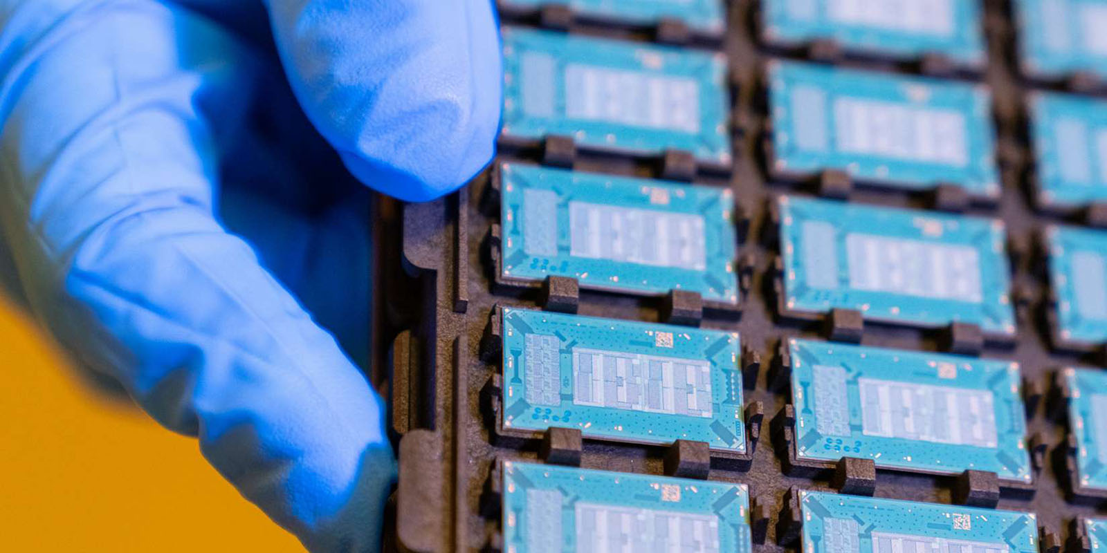
A brand new supply-chain report means that Apple is looking for to be an early participant in what some imagine would be the subsequent huge factor in chip improvement: printed circuit boards (PCBs) constructed from glass substrates.
Whereas that may not sound thrilling, it presents the prospect of a wholly new manner of mounting and packaging chips, which may supply a lot better thermal efficiency, permitting processors to run at most energy for longer durations …
Glass substrates can increase chip efficiency
Present PCBs are sometimes constructed from a mixture of fibreglass and resin beneath the copper and solder layers.
The fabric is delicate to warmth, which signifies that chip temperatures should be fastidiously managed by way of thermal throttling: lowering the efficiency of the chip when it will get too scorching. This implies chips can solely maintain their most efficiency for restricted durations, earlier than falling again to slower speeds to maintain temperatures down.
Switching to glass would considerably enhance the temperatures the board might be subjected to, which in flip signifies that chips can run hotter, and subsequently preserve peak efficiency for longer.
Glass substrates are additionally ultra-flat, permitting for extra exact engraving, which permits parts to be positioned nearer collectively, growing the density of circuits inside any given measurement.
Intel presently holds the lead on this area, however different firms are working onerous to catch up.
Apple in dialogue with suppliers
Digitimes reviews that Samsung is now engaged on this expertise, and that Apple is in dialogue with a number of unnamed suppliers – with Samsung sure to be amongst them.
Subsidiaries of the Samsung Group will collaborate to spend money on the analysis and improvement of Glass Core Substrates (GCS) to expedite their commercialization, aiming to rival Intel, which has taken an early lead on this sector […]
Apple is reportedly in discussions with a number of firms to plot a technique for incorporating glass substrates into digital gadgets. The adoption of glass substrates by Apple sooner or later is predicted to considerably broaden the scope of utility areas.
Sources inside the semiconductor business indicated that cup substrates could grow to be a brand new area for completion amongst nations, attracting participation from world IT gadget producers and semiconductor gamers along with substrate producers.
Samsung is well-placed to work on this, as most of the strategies utilized in manufacturing superior, multilayered shows are additionally relevant to creating glass substrate PCBs.
Doubtlessly the subsequent huge factor, however with challenges
The explanation some imagine that cup substrates would be the subsequent huge factor in chip improvement is that almost all progress so far has been achieved by way of ever-smaller processes. Apple presently leads the best way with the 3nm chip within the A17 Professional powering the iPhone 15 Professional fashions, with plans for 2nm and then 1.4nm.
Every successive course of era is more durable and more durable to realize, with final bodily limits to only how small we are able to go. With doubts as to how lengthy Moore’s Regulation will stay in impact, some imagine that new supplies maintain the important thing to sustaining the tempo of improvement as we start reaching the bounds of course of measurement.
Nevertheless, there are huge challenges forward, as SemiEngineering explains.
“Take into consideration glass as a way to get interconnect density similar to what you’ll get with silicon interposers,” says Rahul Manepalli, fellow and director of substrate TD module engineering at Intel. “A glass substrate provides you that functionality, but it surely comes with very difficult integration and interface engineering issues that we’ve to resolve.”
A few of these challenges embrace fragility, a scarcity of adhesion to metallic wires, and difficulties in attaining uniform through fill, which is essential for constant electrical efficiency. As well as, glass presents distinctive challenges for inspection and measurement, as a result of its excessive stage of transparency and differing reflective indices in comparison with silicon. Many measurement strategies that work on opaque or semi-transparent supplies are much less efficient on glass. For example, optical metrology techniques that depend on reflectivity to gauge distance and depth should adapt to glass’ translucency, which may trigger sign distortion or loss, compromising measurement accuracy.
“All of those applied sciences assume sure physics,” says John Hoffman, pc imaginative and prescient engineering supervisor at Nordson Take a look at & Inspection. “Whenever you begin altering substrates, will the physics nonetheless work? And might you recuperate? A number of our algorithms make sure assumptions in regards to the physics. Do these algorithms nonetheless work, or do we’ve to provide you with model new algorithms as a result of the physics has modified?”
Photograph: Intel
FTC: We use revenue incomes auto affiliate hyperlinks. Extra.