


The photonic chip enhances 5G, AI, and extra, developed by researchers and already impacting telecommunications and tech industries.
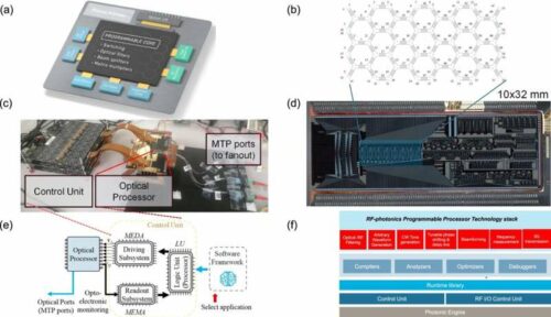
Researchers from the Photonics Analysis Laboratory (PRL)-iTEAM on the Universitat Politècnica de València, in collaboration with the corporate iPRONICS, have developed a groundbreaking photonic chip. This revolutionary chip is designed to be used in telecommunications, information facilities, and synthetic intelligence computing infrastructures. It stands out because the world’s first common, programmable, and multifunctional photonic chip.
This chip will improve a variety of applied sciences together with 5G communications, information facilities, quantum computing, synthetic intelligence, satellites, drones, and autonomous autos, amongst varied different purposes.

The creation of this chip is the first final result of the European mission UMWP-Chip, spearheaded by researcher José Capmany. The findings have been documented within the journal Nature Communications.
The chip developed by the UPV and iPRONICS staff permits on-demand programming and interconnection of wi-fi and photonic segments inside communication networks. This performance helps forestall bottlenecks that may limit each capability and bandwidth.
The researchers clarify that purposes akin to 5G or autonomous vehicles require increased frequencies, which necessitates decreasing the scale of antennas and related circuits. The analysis staff has efficiently developed a converter, an interface chip behind the antenna, that’s as small and compact as attainable, able to help each present and future frequency bands.
The chip has been efficiently built-in into an iPRONICS product referred to as Smartlight, and it has already undergone testing with Vodafone.
“For us, the event of this chip is a vital step as a result of it has allowed the validation of our developments utilized to a rising drawback, the environment friendly administration of information flows in information facilities and networks for synthetic intelligence computing methods. Our subsequent objective is to scale the chip to fulfill the wants of this market phase,” stated Daniel Pérez-López, co-founder and CTO of iPronics.
Assets: Daniel Pérez-López et al, Basic-purpose programmable photonic processor for superior radiofrequency purposes, Nature Communications (2024). DOI: 10.1038/s41467-024-45888-7
Nidhi Agarwal is a journalist at EFY. She is an Electronics and Communication Engineer with over 5 years of educational expertise. Her experience lies in working with improvement boards and IoT cloud. She enjoys writing because it permits her to share her data and insights associated to electronics, with like-minded techies.