


The GaN-based adapter design for energy options. It has a modular setup, is environment friendly, has a large voltage vary, and is straightforward for engineers to customise. Learn extra!
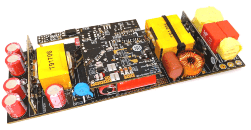
The NCP13992UHD300WGEVB from Onsemi is a GaN-based ultra-high energy density adapter reference design that permits design engineers to create environment friendly, compact energy options. This reference design is a worthwhile device for engineers creating high-performance energy methods with a deal with key parameters like effectivity, no-load enter energy, transient responses, and EMI signature. The design features a Synchronous PFC enhance converter working in Discontinuous Conduction Mode (DCM) or Crucial Conduction Mode (CrM) relying on load and an LLC energy stage with secondary-side synchronous rectification. The NCP1616 controller within the PFC entrance stage ensures a unity energy issue and low enter present THD, whereas the NCP4306 high-performance SR controller synchronizes the PFC enhance SR change.
The LLC stage operates at 500 kHz below nominal load, managed by the NCP13992 current-mode LLC controller. GaN HEMTs in each energy phases preserve excessive effectivity at excessive frequencies. GaN Programs’ GS66504B are used as primary-side switches. The secondary aspect’s synchronous rectifier consists of the NCP4306 controller and two paralleled 60 V energy MOSFETs per department, applied on a devoted SR MODULE daughter card for environment friendly PCB design.

Extremely-high energy density is achieved via the modular design, controllers, drivers, GaN HEMTs, and customized energy magnetics. This guide focuses on the reference design, operation ideas, and connections. For detailed data, confer with the datasheets of the person elements used.
The important thing options of the design embody a GaN HEMT-based design providing ultra-high energy density of as much as 32 W/inch³, a easy two-layer PCB design for all board modules, and a most energy of 300 W with peak energy reaching as much as 340 W at a hard and fast output voltage of 19 V. It helps a large enter voltage vary of 90-265 Vrms, incorporates synchronous CrM PFC utilizing GaN HEMTs, and encompasses a 500 kHz LLC stage with a 600 V HB GaN driver and a high-performance present mode LLC controller. Moreover, it complies with CoC5 Tier 2.
The demo board makes use of a modular system consisting of the primary board and several other daughter-card modules. The next daughter playing cards are inserted into the primary board: bridge rectifier module, CBULK module, LLC stage module and SR module. The modular design affords a number of benefits, together with versatility, the power to check customized daughter playing cards, simple design updates, checking particular person module performance, and house for extra options. This strategy helps scale back PCB space, enhance energy density, and reduce the required PCB layers. All PCBs are designed as two-layer boards with 70 µm copper plating for improved thermal administration and diminished conduction losses, particularly on the secondary aspect, which carries a comparatively excessive output present.
Onsemi has examined this reference design. It comes with a invoice of supplies (BOM), schematics, meeting drawing, printed circuit board (PCB) structure, and extra. The corporate’s web site has further information concerning the reference design. To learn extra about this reference design, click on right here.
👇Comply with extra 👇
👉 bdphone.com
👉 ultractivation.com
👉 trainingreferral.com
👉 shaplafood.com
👉 bangladeshi.assist
👉 www.forexdhaka.com
👉 uncommunication.com
👉 ultra-sim.com
👉 forexdhaka.com
👉 ultrafxfund.com
👉 bdphoneonline.com
👉 dailyadvice.us
