

Courtesy: Lam Analysis
Line edge roughness (LER) is a variation within the width of a lithographic sample alongside one fringe of a construction inside a chip. Line edge roughness could be a vital variation supply and defect mechanism in superior logic and reminiscence units, and might result in poor gadget efficiency and even gadget failure [1~3]. Deposition-etch biking is an efficient approach to cut back line edge roughness. On this research, we reveal how digital fabrication can present steering on tips on how to carry out deposition/etch biking with the intention to scale back LER.
A typical line and through array sample with a pitch of 40 nm was established as a take a look at construction within the digital fabrication software program. Sample vital dimensions (CD) and LER amplitude and correlation size (measures of line edge roughness) have been then explored beneath completely different experimental circumstances.
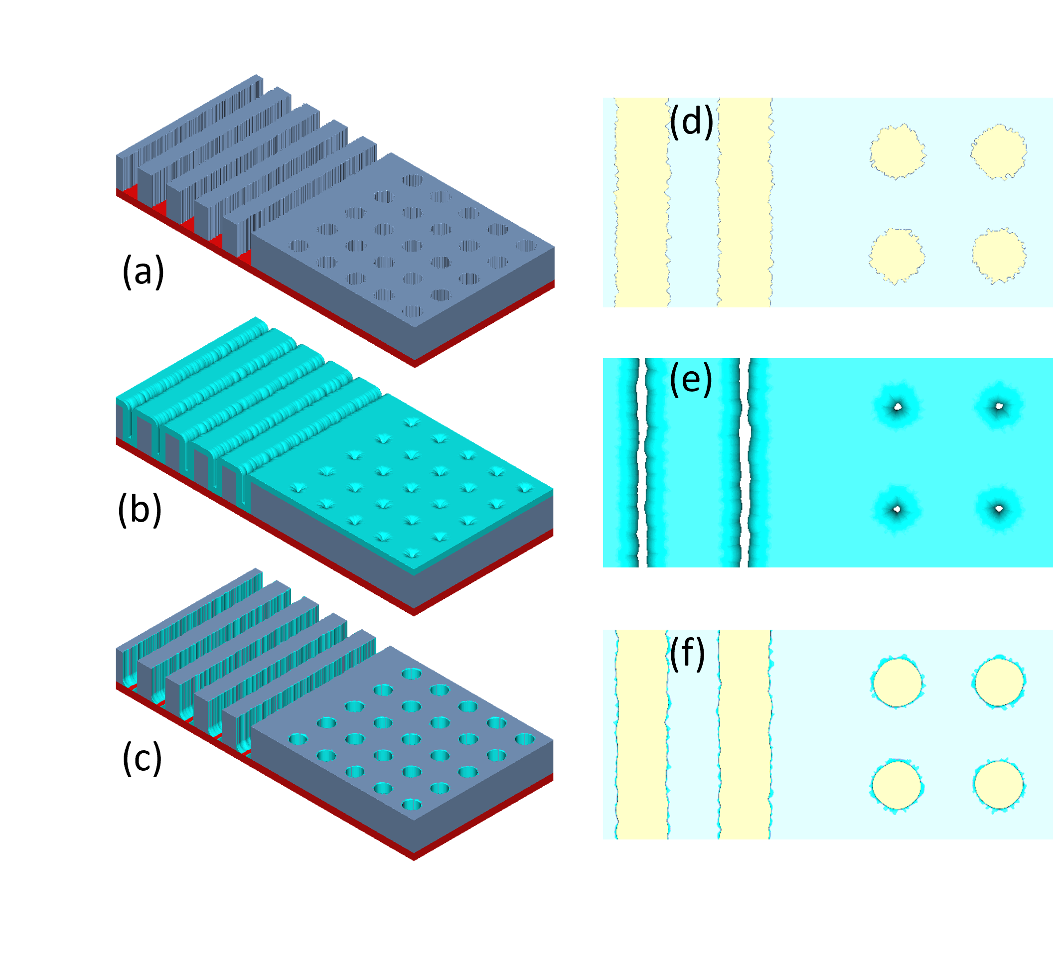
A deposition/etch biking course of was utilized in a digital mannequin to enhance the road edge roughness (LER) and demanding dimension uniformity (CDU) of the sample (Determine 1). Digital metrology was used to measure LER commonplace deviation (LERSTD), LER correlation size (C) and By way of CD vary (VCDR) to guage the affect of the chosen course of modifications on LER and CDU enchancment.
We ran 1,500 digital experiments utilizing the incoming sample CD, LER amplitude (A), LER correlation size (C), etch/deposition quantity (THK), and variety of deposition/etch cycles (NC) as experimental variables. A part of the outcomes of our experiment are proven in Determine 2.
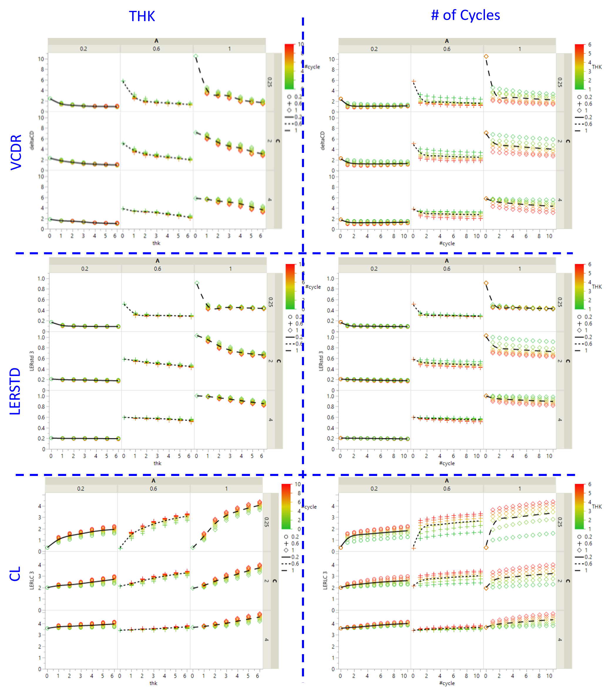
Determine 2 exhibits the pattern within the By way of CD ranges (VCDR), LER commonplace deviation (LERSTD), and LER correlation size (C) values with respect to the variety of deposition / etch cycles (backside axis) at completely different LER A and LER C circumstances (high and proper axis). Our objective is to reduce VCDR, LERSTD and CL values on the lowest variety of deposition / etch cycles. We are able to draw 3 conclusions from Determine 2.
1) Many of the enchancment to LER/VCDR happens within the first deposition/etch cycle.
2) A rise within the deposition quantity (THK, proven in shade on Determine 2) has a better affect on the LER/VCDR enchancment than a rise within the variety of deposition/etch cycles.
3) The LER correlation size (C) turns into bigger after a deposition/etch cycle, however the LER/VCDR enchancment is just not apparent when the LER correlation size (C) will increase.
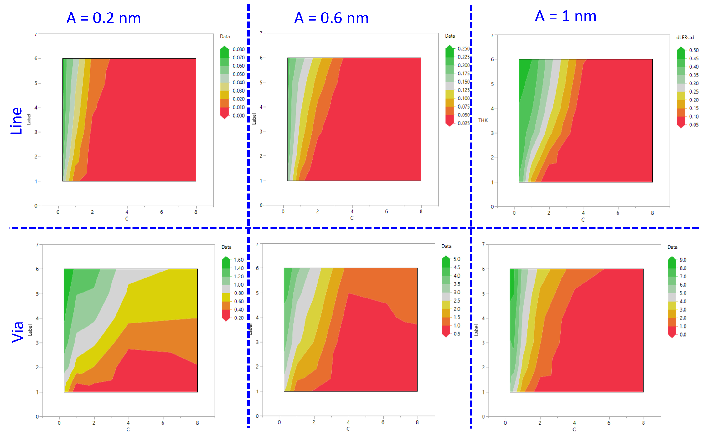
As we talked about earlier, a lot of the LER enchancment occurred within the first deposition/etch cycle, with the remaining deposition/etch cycles producing a a lot smaller enchancment. Contour plots displaying the LER/VCDR enchancment on the 1st cycle was fitted and illustrated in Determine 3. From Determine 3, we will draw 2 conclusions:
1). Though much less enchancment was seen with a bigger incoming LER correlation size (C), enchancment nonetheless occurred on the through patterns if a thicker movie was used through the deposition portion of the cycle when there was a bigger LER correlation size (LER C) and decrease LER amplitude (LER A).
2). LER/VCDR might be improved utilizing a comparatively thicker deposition movie at bigger incoming LER C circumstances.
On this research, a deposition/etch biking course of was simulated to enhance LER and CDU efficiency at superior nodes by digital fabrication. The outcomes point out that a lot of the LER/VCDR enchancment seen throughout deposition/etch biking processes occurred through the first deposition/etch cycle. The deposition/etch biking course of may be very efficient in decreasing excessive frequency noise (when there’s a smaller LER correlation size). LER enhancements are bigger on the through patterns than on the line patterns when a thicker movie is deposited, exhibiting as bigger LER correlation size values and decrease LER amplitude. These outcomes present quantitative steering on the optimum collection of deposition/etch quantities and the variety of cycles wanted, to each scale back LER and decrease defects and variability within the manufacturing of superior semiconductor units.
👇Comply with extra 👇
👉 bdphone.com
👉 ultraactivation.com
👉 trainingreferral.com
👉 shaplafood.com
👉 bangladeshi.assist
👉 www.forexdhaka.com
👉 uncommunication.com
👉 ultra-sim.com
👉 forexdhaka.com
👉 ultrafxfund.com
👉 ultractivation.com
👉 bdphoneonline.com