


Littelfuse p-channel energy MOSFETs, though much less famend than their extensively used n-channel counterparts, have historically served a restricted vary of purposes. Nevertheless, with the rising demand for low-voltage (LV) purposes, the scope of p-channel energy MOSFETs has been expanded. The simplicity of making use of Littelfuse p-channel options for high-side (HS) purposes makes them extra enticing for LV inverters (< 120 V) and non-isolated point-of-load options. The convenience of driving an HS p-channel MOSFET with out the necessity for a cost pump or extra voltage supply leads to simplified designal, area financial savings, decreased half depend and price effectivity.
This text makes a primary comparability of n-channel and p-channel energy MOSFETs, introduces Littelfuse’s p-channel energy MOSFETs, after which explores their goal purposes.
A comparative evaluation of n-channel and p-channel energy MOSFETs
To attain the identical on-state resistance RDS(on) because the n-channel kind MOSFET, the p-channel requires a 2 to 3-times bigger die measurement. Due to this fact, in high-current purposes, the place low conduction losses are essential, massive die p-channel MOSFETs with very low RDS(on) are suboptimal. Whereas the bigger chip measurement of the p-channel system provides improved thermal efficiency, it displays bigger intrinsic capacitances and thus increased switching losses. This disadvantage considerably impacts total system value, effectivity, and thermal administration when the system operates at a excessive switching frequency.


In low-frequency purposes with important conduction losses, a p-channel MOSFET ought to match the RDS(on) of an n-channel MOSFET, requiring a bigger chip space. Conversely, in high-frequency purposes prioritizing switching losses, a p-channel MOSFET ought to align with the entire gate prices of an n-channel counterpart, usually having an identical chip measurement however a decrease present score. Due to this fact, selecting the best p-channel MOSFET calls for cautious consideration of system RDS(on) and gate cost (Qg) specs together with the thermal efficiency.
Littelfuse p-channel energy MOSFETs
Littelfuse provides a spread of business certified p-channel energy MOSFETs with the very best voltage class, lowest RDS(on) and Qg, excessive avalanche vitality score, wonderful switching efficiency and superior secure working space (SOA) with best-in-class efficiency in each normal industrial and distinctive remoted packages. Littelfuse p-channel energy MOSFETs retain the important options of comparable n-channel energy MOSFETs similar to quick switching, environment friendly gate-voltage management, and wonderful temperature stability.
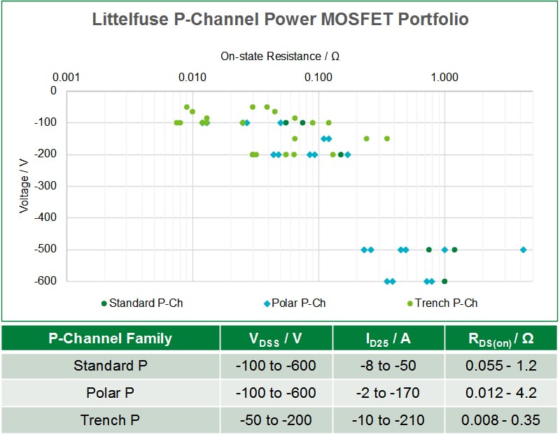
Fig. 2 presents the important thing highlights of p-channel energy MOSFETs provided by Littelfuse. Customary P and PolarP™ planar gadgets can be found with voltage scores from -100 V to -600 V and present scores from -2 A to -170 A. PolarP™ provides optimized cell construction with low area-specific on-state resistance and improved switching efficiency, whereas Customary P advantages from a greater SOA efficiency. Trench P using a extra dense trench gate cell construction provides very low RDS(on), low gate cost, quick physique diode and quicker switching with system voltages starting from -50 V to -200 V and currents from -10 A to -210 A. The most recent addition to the portfolio is IXTY2P50PA (-500 V, -2 A, 4.2 Ω) which is Littelfuse’s first automotive grade p-channel energy MOSFET for automotive purposes.
Functions for Littelfuse p-channel energy MOSFETs
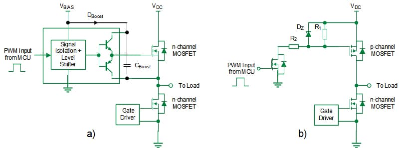
N-channel MOSFETs are sometimes used within the energy stage in typical half-bridge (HB) purposes, . Nevertheless, n-channel HS switches necessitate a bootstrap circuit to generate a gate voltage that’s floating close to the supply of the HS MOSFET or an remoted energy provide to activate as proven in Fig. 3a). Therefore, the benefit of utilizing n-channel gadgets comes at the price of elevated complexity in gate driver design resulting in extra design effort and higher area utilization. Fig. 3 illustrates the distinction between circuits utilizing complementary MOSFETs and people utilizing n-channel MOSFETs. When a p-channel MOSFET is used because the HS change on this configuration as depicted in Fig. 3b), it may possibly vastly simplify the motive force design. A cost pump that drives the HS change may very well be eliminated and the p-channel MOSFET will be simply managed by the MCU by means of a easy stage shifter. This reduces design effort and half quantity depend leading to a cost-efficient design that makes use of area effectively.
Reverse polarity safety
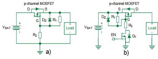
Reverse polarity safety is a security measure inside programs to stop potential hearth hazards and damages brought on by a reverse connection of the facility supply. Fig. 4a) exhibits the reverse polarity safety carried out utilizing a p-channel energy MOSFET. When the battery is accurately related, the intrinsic physique diode conducts till the MOSFET channel is activated. Within the occasion of a reverse connection of the battery, the physique diode is reverse-biased, with the gate and supply on the identical potential, thereby turning off the p-channel MOSFET. A Zener diode clamps the gate voltage of the p-channel MOSFET, defending it in case of excessively excessive voltage ranges.
Load change
Load switches join or disconnect a voltage rail to a selected load providing a cheap and easy approach for a system to effectively handle energy. Fig. 4b) demonstrates a circuit utilizing a p-channel energy MOSFET for a load change. This circuit is pushed by a logic allow (EN) sign controlling the p-channel load change by way of a small-signal n-channel MOSFET Q1. When EN is low, Q1 is off, and the p-channel gate is pulled as much as VBAT. Conversely, when EN is excessive, Q1 prompts, grounding the p-channel gate, and turning on the load change. If VBAT exceeds the p-channel MOSFET’s threshold voltage, it may possibly activate when EN is excessive, eliminating the necessity for an extra voltage supply to bias the gate, which is important for n-channel MOSFETs. The collection resistor is required to restrict the present and a Zener Diode to clamp the gate voltage to a most worth.
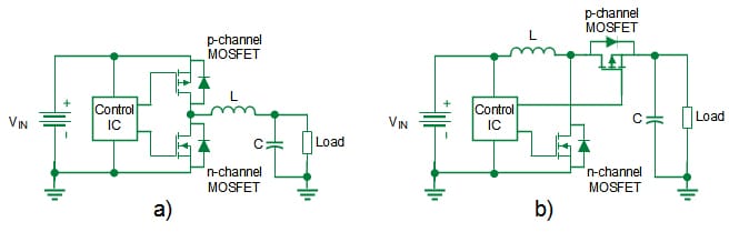
DC-DC converters
Conclusion
With the event of contemporary LV purposes, Littelfuse’s p-channel energy MOSFETs show their versatility in assembly the evolving wants of right now’s energy electronics. Using Littelfuse’s complete vary of p-channel MOSFETs gives designers with benefits similar to simplified, extra dependable, and optimized circuit design in industrial and automotive purposes. To attain optimum efficiency for particular purposes, designers should assess the trade-off between RDS(on) and Qg when deciding on a p-channel energy MOSFET.
Creator: Sachin Shridhar Paradkar, Littelfuse