


Uncover the driving forces behind the semiconductor revolution—how AI slashes human error, finds untapped income streams, and underscores the pivotal function of customisation with domain-specific chipsets.
The surge in demand for synthetic intelligence (AI) and the Web of Issues (IoT) gadgets is reshaping how we work together with know-how and the world round us. From good trackers in our watches to clever thermostats in our houses, the applying of synthetic intelligence (AI) is permeating each side of our lives. A shopper survey predicts that by 2030, we might be surrounded by greater than 350 billion AI IoT gadgets, underlining the fast development in demand for these gadgets.

Whereas the proliferation of AI IoT gadgets is spectacular, it additionally raises questions in regards to the function of AI in bettering our lives and the potential for human error in these applied sciences. On this article, we are going to discover the important thing traits in AI purposes, the necessity for elevated computational energy, and the driving brokers behind this revolution within the semiconductor business.

AI purposes and decreasing human error
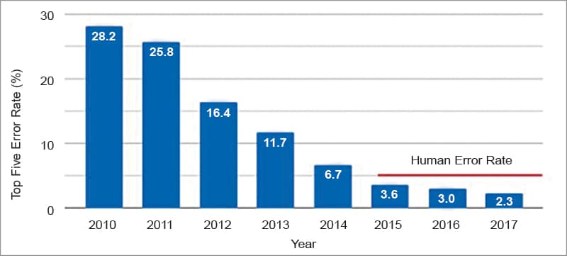
The first purpose of integrating AI into IoT gadgets is to reinforce their capabilities and scale back human error. AI can present extra correct outcomes than the human eye or persistence in numerous purposes, reminiscent of picture recognition. As an example, due to machine computing energy, Google’s picture recognition software considerably lowered human error charges when AI was utilised. Because of this, there’s a rising want for complicated system-on-chip (SoC) architectures to help these AI use instances. These architectures should evolve to accommodate single-threaded purposes, OpenCL help, benchmarking, multi-threaded networking purposes, and picture recognition.
In networking purposes, focus lies in leveraging community perform processors to reinforce system efficiency. One important side that has been emphasised is safety, primarily as a result of huge knowledge transmitted between edge gadgets and cloud companies. We should make sure the integrity and authenticity of this knowledge alongside its journey.
We’re actively implementing strong computing mechanisms throughout the communication channel to realize this. These mechanisms are designed to confirm and validate knowledge integrity at each the sting and cloud endpoints. Guaranteeing the info’s accuracy is paramount, guaranteeing that the knowledge transmitted aligns with the meant content material.
| Key driving brokers in semiconductor evolution |
| A number of key driving brokers have performed important roles in shaping the semiconductor business through the years: Expertise shift in AI compute necessities • The semiconductor business experiencing a know-how shift attributable to rising demand for AI purposes • OEM producers and chip design groups engaged in software benchmarking to evaluate computational energy capabilities • AI integration into every day life necessitates {hardware} adaptation to satisfy elevated calls for Surge in demand for sub-micron compute gadgets • Computer systems are shrinking in measurement whereas computational calls for are on the rise, making a paradox • Creating sub-micron computing gadgets and manufacturing applied sciences is important to handle this problem • Trade should help smaller but extra highly effective gadgets, scale back prices, and guarantee reliability The function of extra (reliability, stability, and energy effectivity) • Semiconductor engineers face reliability, stability, and energy consumption challenges in sub-micron know-how • Growing the transistor depend on chips necessitates sustaining high-reliability requirements • Guaranteeing reliability is significant for the seamless operation of AI-powered gadgets These driving brokers proceed to form the semiconductor business, with developments in chip design, manufacturing, and purposes resulting in ever extra highly effective and environment friendly digital gadgets. |
The pursuit extends to fulfilling the computational calls for related to picture recognition. This necessitates environment friendly computing assets to analyse and course of visible knowledge, additional enhancing the capabilities and worth of our networking purposes. Firms like Nvidia are on the forefront of offering the mandatory computational energy to satisfy these calls for.
Automation within the semiconductor lifecycle
Automating the semiconductor lifecycle is one other essential side of the AI revolution within the business. McKinsey’s analysis means that AI might generate $85 billion to $95 billion in income over the long run, highlighting the untapped potential of AI-driven automation in semiconductor manufacturing. As AI methods turn out to be extra superior, semiconductor corporations embrace them to streamline processes and enhance operational efficiencies.
The AI revolution is reshaping the semiconductor business in profound methods. The demand for AI IoT gadgets is driving the necessity for elevated computational energy, sub-micron compute gadgets, and extra dependable semiconductor designs. Moreover, the automation of the semiconductor lifecycle by means of AI guarantees important income potential. As we proceed integrating AI into our every day lives, the semiconductor business will play a pivotal function in supporting these technological developments, in the end shaping the way forward for our interconnected world.
The semiconductor business is not any stranger to innovation and adaptation. To satisfy the calls for of AI purposes, it’s essential to evaluate whether or not our chipsets can help numerous AI duties successfully. Benchmarking is pivotal on this exploration, evaluating AI accelerators throughout completely different chipsets by measuring ‘TOPs’ (tera operations per second).
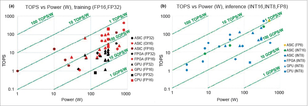
TOPS is a simplifying metric
TOPS tells you what number of computing operations an AI accelerator can deal with in a single second at 100% utilisation. In essence, it appears at what number of math operation issues an accelerator can resolve in a really brief interval.
What’s attention-grabbing to notice is that scalability in chip design shouldn’t be at all times linear. Growing computational energy by merely including extra cores or capability doesn’t assure a proportional enhance in efficiency. This highlights the significance of rigorous architectural exploration and benchmarking operations to make sure that AI purposes will be dealt with effectively by {hardware}.
Simple development in AI {hardware} design
Linear scalability shouldn’t be as simple as it could appear. Merely rising system-on-chip (SoC) capability and compute energy doesn’t essentially equate to a proportional enhance in computational functionality. This very important message underscores the necessity for a deeper exploration of system structure and complete benchmarking operations to make sure our {hardware} successfully handles AI purposes.
Initially, the prevailing knowledge amongst system designers was that increasing compute energy primarily concerned ramping up the variety of CPUs and cores to realize most efficiency. Nonetheless, modern benchmarking efforts have revealed that this method doesn’t yield a direct and flawless linear scaling. Growing the variety of cores, whereas helpful to a sure extent, encounters limitations associated to energy consumption and different systemic architectural constraints.
To satisfy the calls for of AI purposes, it’s crucial that we delve into different aspects of system design. This shift in perspective is essential to facilitate the seamless transition of our {hardware} to accommodate numerous use instances. For many people on this discipline, this shift in pondering is of private curiosity. It brings into focus the essential significance of software benchmarking in assessing the general system design.
The search for optimum options extends past mere processing energy and touches upon the intricacies of energy effectivity, architectural design, and the various wants of AI purposes. On this journey, time to market stays a big consideration. Complicated software benchmarking has turn out to be an integral a part of our technique as we try to bridge the hole between {hardware} capabilities and the evolving calls for of AI purposes. By means of these efforts, we purpose to make sure that our {hardware} is not only conserving tempo however main the best way within the dynamic realm of AI know-how.
Customisation and domain-specific chipsets
Historically, semiconductor designers aimed to extend compute energy by including extra general-purpose CPUs and cores. Nonetheless, as benchmarking has proven, there are limits to this method, constrained by elements like energy consumption and system architectural limitations. This realisation has led to a shift in direction of domain-specific chipsets.
In the present day, chipsets will be designed to serve particular domains or purposes. Somewhat than a one-size-fits-all method, these domain-specific chipsets will be tailor-made to the distinctive necessities of various purposes, reminiscent of net looking, minimal purposes, multimedia, picture recognition, and extra. This customisation permits chipsets to be extra environment friendly and cost-effective, assembly the precise wants of every software.
One of the crucial thrilling developments in semiconductor design is the emergence of software-defined {hardware}. This paradigm shift recognises that whereas general-purpose chipsets have their place, the long run lies in customized, adaptable chips designed for particular duties.
Software program-defined {hardware} permits chip designers to create modules that may be activated or deactivated relying on the applying’s necessities. This flexibility ensures that the chip stays power-efficient and able to delivering excessive efficiency for the meant activity. It’s a revolutionary method that addresses the dynamic wants of the trendy AI panorama.
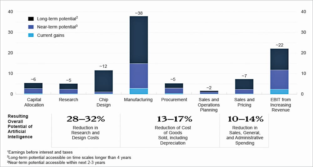
Past chip design, AI is making important inroads into all the semiconductor lifecycle. McKinsey’s analysis means that AI can play an important function in numerous levels, from capital allocation and product portfolio definition to chip design and provide chain administration.
AI-driven automation guarantees to streamline processes, enhance operational efficiencies, and scale back prices. For instance, Google’s open chip structure leverages AI to design chipsets, demonstrating the potential of AI in semiconductor design. Moreover, AI can optimise provide chain operations, mitigating points like the availability chain disruptions skilled throughout the Covid-19 pandemic.
The semiconductor business is on the cusp of a revolution pushed by AI and customisation. Because the demand for AI-powered gadgets continues to develop, semiconductor designers should adapt to satisfy the various wants of various purposes effectively. Software program-defined {hardware}, domain-specific chipsets, and AI-driven automation are key traits that can form the business’s future.
Recognising the strategic significance of AI and expertise improvement, semiconductor corporations are embracing AI as a high precedence. The Worldwide Expertise Roadmap for programs and gadgets (IEEE) can also be actively contributing to the ecosystem’s improvement. The semiconductor business’s transformation is inevitable, and people who harness the facility of AI and customisation will thrive on this new period of semiconductor design and know-how.
The semiconductor business is within the midst of a transformative period, pushed by the combination of AI and the rising demand for customisation. In a current dialogue, business specialists explored the assorted aspects of this revolution, from customized chipsets to software-defined {hardware} and the function of AI in reshaping semiconductor design and improvement. On this article, we are going to take a more in-depth have a look at the insights and improvements shared throughout this enlightening dialog.
AI’s function and customisation with ASICs and domain-specific chipsets
Software-specific built-in circuits (ASICs) and domain-specific chipsets, because the title suggests, are designed with a particular software or use case in thoughts. These chips are tailor-made to excel of their meant software, whether or not AI for autonomous autos or industrial automation.
What’s noteworthy is that these ASICs will not be one-size-fits-all options. As an alternative, they’re finely tuned to satisfy the distinctive necessities of every software, leading to improved effectivity and cost-effectiveness. This transfer in direction of customisation is altering the sport in semiconductor design, permitting corporations to supply specialised chipsets that cater to numerous industries and purposes.
The software-defined {hardware} challenges the normal method of fastened {hardware} configurations. As an alternative, it introduces flexibility by enabling modules inside a chip to be activated or deactivated relying on the precise software’s wants.
For instance, think about a Tesla automobile. Clients can buy a base mannequin after which select to allow extra options or functionalities as wanted. These options are already current within the {hardware}, however they are often unlocked by means of software program activation. This method permits for larger adaptability and effectivity in {hardware} utilization.
AI is making its mark all through the semiconductor lifecycle. One notable software of AI is in creating information bases and chatbots to assist in post-silicon ramp-up. Semiconductor engineers face the problem of quickly buying numerous talent units as they work on chips for various purposes. To streamline this studying course of, corporations are utilizing AI-driven chatbots to supply engineers with fast entry to coaching supplies, knowledge, and insights, serving to them ramp up extra effectively.
Within the pre-silicon part, AI is proving invaluable within the realm of security simulations. Within the automotive business, security is paramount, and AI simulations are getting used to check and confirm chip performance in essential security eventualities. This ensures that chips meet the stringent security requirements for purposes like autonomous autos.
Untapped income potential
By integrating AI into numerous features of the semiconductor course of, corporations can enhance operational efficiencies, scale back prices, and create new income streams. As an example, AI can optimise capital allocation, improve product portfolio definition, help in chip design, and streamline provide chain administration.
The McKinsey and Firm research means that embracing AI in semiconductor improvement might yield important returns, with potential financial savings starting from 28% to 32% of design prices. These findings underscore the compelling enterprise case for AI adoption within the semiconductor business.
The semiconductor business is profoundly reworking, with AI and customisation on the forefront of innovation. From ASICs and domain-specific chipsets to software-defined {hardware} and AI-driven automation, the business is embracing change to satisfy the calls for of a dynamic and interconnected world. As AI continues to reshape semiconductor design and improvement, corporations that leverage its energy and adapt to the evolving panorama might be well-positioned for fulfillment on this thrilling period of semiconductor know-how.
Area-programmable gate arrays (FPGAs) supply builders the power to outline customized purposes and modules throughout the chip, offering flexibility and adaptableness for iterative improvement and testing. However, the SoC method fabricates chips particularly for a selected software, optimising {hardware} for effectivity and efficiency. Developments like five-nanometre know-how in SoCs allow extra complicated computations.
The combination of AI into the semiconductor business is additional driving innovation, optimising {hardware}, enabling software-defined upgrades, and bettering post-silicon information bases. These developments promise an thrilling future for customized purposes and chip design.
It turns into evident that we’re on the point of a transformative period. The demand for AI IoT gadgets is propelling the business to innovate at an unprecedented tempo, requiring elevated computational energy, domain-specific chipsets, and software-defined {hardware}. AI’s integration into all the semiconductor lifecycle guarantees operational efficiencies and important value financial savings.
The way forward for semiconductor design and know-how is being formed by AI and customisation, and people who adapt will thrive on this dynamic panorama. As we proceed to witness the seamless integration of AI into our every day lives, it’s clear that the semiconductor business holds the important thing to unlocking the limitless prospects of a extra interconnected and clever world.
This text relies on a tech speak session at EFY Expo 2023, Delhi, by Balvinder Khurana, Senior Engineering Supervisor System Validation, NXP. It has been transcribed and curated by Akanksha Sondhi Gaur, Analysis Analyst and Journalist at EFY.
👇Observe extra 👇
👉 bdphone.com
👉 ultraactivation.com
👉 trainingreferral.com
👉 shaplafood.com
👉 bangladeshi.assist
👉 www.forexdhaka.com
👉 uncommunication.com
👉 ultra-sim.com
👉 forexdhaka.com
👉 ultrafxfund.com
👉 ultractivation.com
👉 bdphoneonline.com