

System engineers designing high-power functions akin to electrical automobiles, industrial drives and pumps, and uninterruptible energy provides are selecting Silicon Carbide (SiC) MOSFETs due to the improved effectivity and elevated energy density SiC know-how offers over IGBTs. To keep up total system effectivity and cut back energy loss, it’s important to pair the best SiC gate driver alongside these MOSFETS.
This weblog explains the significance of system energy effectivity and offers a quick tutorial on the standards you have to think about when choosing a SiC gate driver, together with SiC energy dissipation, SiC turn-on and off fundamentals, and find out how to cut back switching losses. We additionally introduce the NCP(V)51752, a first-of-its-kind 3.75 kV gate driver with built-in unfavorable bias.
Each Milli-P.c Issues
In relation to managing energy loss, for high-power functions starting from 10s of kW to megawatts, each milli-percent of effectivity matter. For instance, a 100 W utility working at 95% effectivity leaves solely 5 W of energy dissipation to be managed by your cooling technique. In brief, you would add a heatsink, and possibly a fan, and also you’re good to go. However a 350-kW utility working on the identical effectivity yields 17.5 kW of energy dissipation, requiring important engineering and value for managing your cooling technique, to not point out your carbon footprint.
Lowering Energy Losses
The entire energy loss exhibited by SiC is basically the sum of the conduction losses plus the switching losses. SiC conduction losses are dominated by I2R, the place I is the drain present (ID) and R is the RSDON or the resistance of the Drain to Supply present path when the SiC MOSFET is totally turned on. System engineers can design for very low conduction losses by selecting low RDSON SiC MOSFETs, configuring a number of SiC MOSFETs in parallel, or each.
SiC switching losses are extra sophisticated, influenced by parameters just like the Complete Gate Cost (QG(TOT)), the Reverse Restoration Cost (QRR), Enter Capacitance (CISS), Gate Resistance (RG), EON losses and EOFF losses, to call just a few.
QG(TOT), Complete Gate Cost
The Complete Gate Cost QG(TOT) is the quantity of cost (Coulombs) that the gate driver must inject into the gate electrode to show the MOSFET totally on or off. Usually, the QG(TOT) is inversely proportionate to the RDSON. So, as system engineers choose decrease RDSON SiC MOSFETs to scale back conduction losses of their high-power functions, the gate drive supply (activate) and sink (flip off) present necessities enhance proportionally.
System design for decrease switching losses turns into fairly difficult as a result of, on one hand, you need to activate and off as rapidly as doable to reduce switching losses. However then again, sooner switching speeds can introduce undesirable electromagnetic interference (EMI), in addition to probably harmful and unintended parasitic turn-on throughout supposed swap turn-off, particularly in half-bridge topologies.
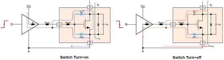
Flip-On and Flip-Off
To function a MOSFET and begin conduction, a voltage should be utilized to the gate terminal that’s relative to the supply terminal. Devoted drivers are used to use voltage and supply drive present to the gate of the ability machine. The gate driver serves to show the ability machine on and off by sourcing or sinking the drive present, respectively. So as to take action, the gate driver expenses the gate of the ability machine as much as its last flip−on voltage, VGS(ON), or the drive circuit discharges the gate right down to its last flip−off voltage, VGS(OFF). The transition between the 2 gate voltage ranges requires a certain quantity of energy to be dissipated within the loop between the gate driver, gate resistor, and energy machine.
Right this moment, excessive−frequency converters for low- and medium-power functions are predominantly making use of energy MOSFETs. Nonetheless, gate drivers aren’t just for MOSFETs, however they’re additionally ideally appropriate for comparatively new and esoteric units from the vast band hole group akin to SiC MOSFETs and GaN (gallium nitride) MOSFETs. The place larger driving present is required for quick ON/OFF energy switching, the best-performing units in use right now are normally SiC MOSFETs.
Parasitic Flip On
Due to the very excessive di/dt, extreme ringing can happen when the gate driver reaches the minimal Gate to Supply Voltage. That is compounded by parasitic capacitances and inductances augmented by PCB format and packaging, inflicting inductive kicks throughout flip off. These inductive kicks can inadvertently journey the VGS(TH) inflicting an unintended activate throughout supposed flip off, which might set off disastrous outcomes. For instance, think about a half bridge utility. When the low aspect swap is turned off and the excessive aspect swap is about to be turned on, low aspect swap could be accidently turned on (VGS(TH) tripped by inductive kick), inflicting each the excessive aspect and low aspect switches to be concurrently turned on (shoot-through present). This will likely lead to a direct brief from the excessive voltage rail to floor, which might trigger harm to the MOSFET. One very efficient mitigation towards this challenge is to swing under 0V, right down to -3V and even -5V throughout flip off, creating some headroom or margin towards this unintended inductive kick tripping the VGS(TH).
Switching Losses
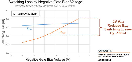
The plot in Determine 2 (supply: AND90204/D), the place the x-axis captures the Unfavorable Bias Flip off voltage from 0V to -5V, and the y-axis captures switching losses (µJ), illustrates the second benefit for unfavorable bias flip off leading to lowered EOFF switching losses. In reality, by reducing the flip off voltage from 0V to -3V when driving onsemi’s Gen 2 “M3S” sequence of SiC MOSFETS designed particularly for prime switching frequency functions, switching losses could be lowered by as a lot as 100 uJ. An EOFF discount from 350 µJ at 0V to 250 µJ at -3V unfavorable bias turn-off yields 25% discount in EOFF losses. And keep in mind, each milli-percent issues!
Gate Drive Flip Off with Built-in Unfavorable Bias
onsemi presents many excessive voltage, excessive energy remoted SiC gate drivers that help “exterior unfavorable bias” throughout turn-off, the place the system provides the -3V or -5V to the gate driver to generate the unfavorable swing.
The NCP(V)51752 is a brand new household of remoted SiC gate drivers that includes inside unfavorable bias.
This characteristic saves system prices as a result of the system doesn’t have to provide the unfavorable bias rail to the gate driver – the NCP(V)51752 does it by itself.
The 4 under trim choices of the NCP(V)51752 can be found. Different choices can be found on demand.
- NCP51752CDDR2G: Industrial, UVLO: 12V, Unfavorable Bias: -5V
- NCP51752DBDR2G: Industrial, UVLO: 17V, Unfavorable Bias: -3V
- NCV51752CDDR2G: Automotive, UVLO: 12V, Unfavorable Bias: -5V
- NCV51752CBDR2G: Automotive, UVLO: 12V, Unfavorable Bias: -3V
Conclusion
The NCP(V)51752, 3.75kV, 4.5A/9A, Galvanic Remoted (enter to output), Single Channel SiC Gate Driver with built-in unfavorable bias:
- Mitigates towards unintended turn-on throughout supposed turn-off.
- Reduces EOFF switching losses by 25%.
- Saves system prices.
👇Observe extra 👇
👉 bdphone.com
👉 ultraactivation.com
👉 trainingreferral.com
👉 shaplafood.com
👉 bangladeshi.assist
👉 www.forexdhaka.com
👉 uncommunication.com
👉 ultra-sim.com
👉 forexdhaka.com
👉 ultrafxfund.com
👉 ultractivation.com
👉 bdphoneonline.com