

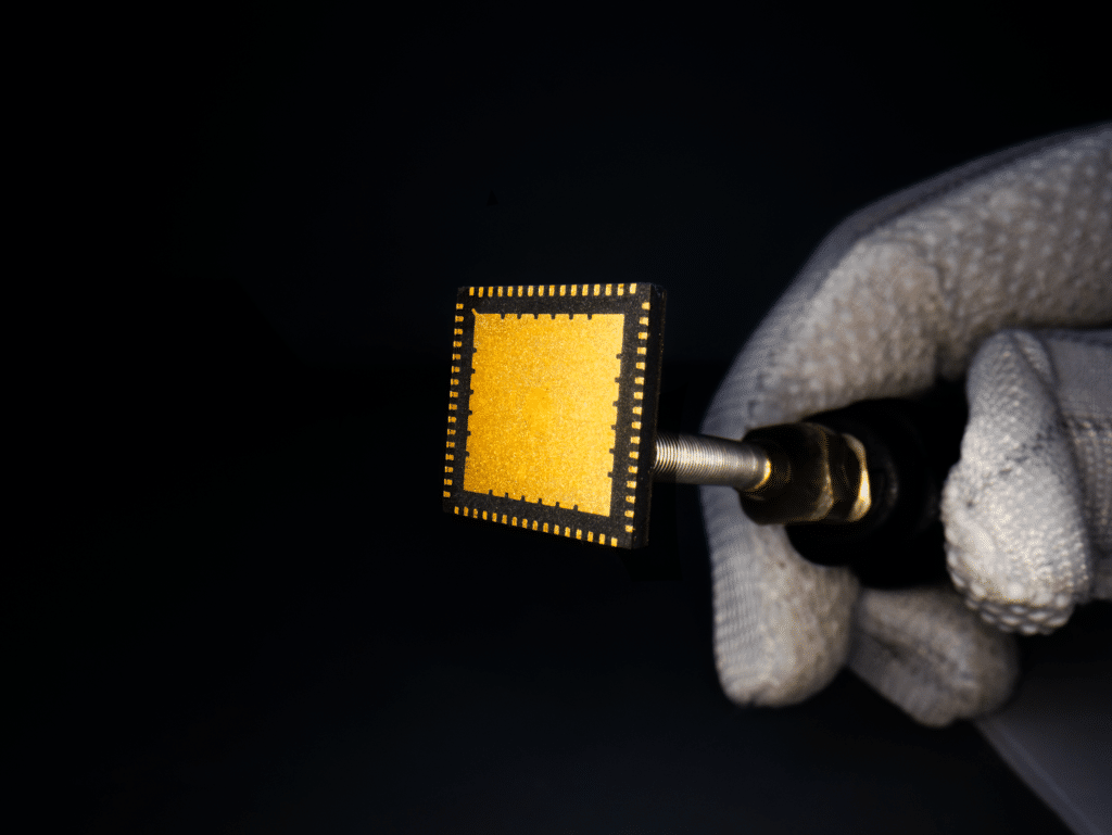
The Chennai-based startup has accomplished the prototype fabrication of the IoT Microcontroller and can quickly roll out the reference boards.
Semiconductor fabless startup Mindgrove Applied sciences is about to roll out India’s first 700 MHz high-performance microprocessor, Safe IoT, for linked gadgets, particularly these requiring enhanced safety on the chip stage.
Out of the corporate’s first hundred prototypes, ten are already present process practical testing, and the rest are set to reach within the coming weeks.

With a tagline ‘designed in India, designed for the world’, co-founders T.R. Shashwath and Sharan Jagathrakshakan are concentrating on Indian designers and are presently engaged in high-level discussions with corporations within the client home equipment phase. “The market extends past the nation’s borders, as many merchandise are exported globally,” provides Shashwath.
Powered by the Shakti C-Class processor developed at IIT Madras, Safe IoT’s underlying RISC-V structure contains a compressed instruction set built-in with the primary instruction set. This reduces instruction measurement whereas sustaining compatibility and interplay with different directions.
“On condition that customers are prone to redesign their methods, we’ve opted for a 64-bit, 700 MHz frequency operation as an alternative of the 32-bit low-frequency operation to make sure future-proofing for upcoming functions, prioritizing greater efficiency,” co-founder Sharan instructed EFY.
The chip combines its processing capabilities with an influence consumption of underneath 200mW, making it perfect for a lot of functions requiring prolonged battery life, together with good locks, watches, utility meters, thermal printers, followers, biometric modules, and extra.
The startup gives in depth peripheral help for higher connectivity and interoperability with its 96 practical I/O pins and varied communication interfaces. “As a designer, I detest being compelled to decide on between peripherals attributable to multiplexing!” says Shashwath.
The startup has minimized multiplexing to incorporate solely PWMs, whereas all the things else has devoted I/O pins. “We provide 4 unbiased SPIs, two unbiased quad SPIs, three unbiased UART ports, and 32 GPIOs. Each quad SPIs are memory-mapped as much as 512 megabytes every, facilitating high-performance microcontroller functions with in depth reminiscence maps. This simplifies the design course of for customers, permitting for versatile module configurations,” elaborates Shashwath.
The chip’s design integrates on-board safety features, together with built-in crypto accelerators and FIPS-140-2 licensed OTP and TRNG, making certain end-to-end encryption and safety towards potential safety threats. “Our chip contains an AES 256 accelerator, RSA 2048, a devoted one-time programmable reminiscence separate from flash, and a pre-certified true random quantity generator important for encryption. These safety features have been initially developed at IIT Madras, open-sourced, and later enhanced for deployment on our chip,” reveals Sharan.
The chip helps varied working methods and IDEs, together with Zephyr, FreeRTOS, NuttX, Eclipse, and VSCode. “We presently don’t provide out-of-the-box help for commercial-grade OS like QNX, as we haven’t but developed the aptitude to port them. Nonetheless, if a buyer requests help for QNX or another OS, we’re open to collaborating as our silicon helps customary RISC-V extensions, making the porting course of comparatively simple,” explains Sharan.
The startup’s help extends past {hardware} and software program, together with analysis boards, stamp modules, and reference designs for higher integration and deployment.