


Researchers achieved a exact fabrication technique of 2D semiconductors for CMOS inverters array.
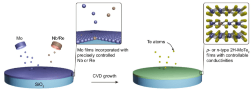
A group of researchers from Peking College, China have created a way for exactly doping two-dimensional (2D) semiconductors. Utilizing substitutional doping, the group efficiently synthesised skinny movies of 2H-MoTe2 with P-type and N-type areas, enabling the fabrication of a chip-sized 2D CMOS inverter array. This achievement represents a major step towards revolutionising built-in circuit expertise.
Exact doping performs a important function in semiconductor fabrication, figuring out the conductivity and performance of units. Whereas conventional doping strategies like ion implantation are well-suited for bulk supplies akin to silicon, they’re incompatible with atomically skinny 2D semiconductors. This examine overcomes that limitation, demonstrating a scalable strategy to doping 2D supplies with unparalleled precision.

The researchers used magnetron sputtering and chemical vapour deposition methods to include niobium (Nb) and rhenium (Re) into 2H-MoTe2 movies. The ensuing P- and N-type channels have been then used to assemble back-gate and CMOS units. Corridor measurements revealed distinct doping traits: Nb-doped movies exhibited p-type behaviour, whereas Re-doped movies displayed ambipolar and N-type traits, relying on doping ranges. These findings affirm the high-quality synthesis and managed provider concentrations of the doped movies.
This innovation targets semiconductor producers and researchers exploring next-generation electronics. The compatibility of the tactic with large-scale fabrication was demonstrated by producing tons of of CMOS inverter arrays on centimetre-scale chips. By attaining reproducible doping and integrating P- and N-type movies, the examine highlights the potential for scalable manufacturing of superior digital units.
“This technique permits for spatially selective doping with outstanding accuracy, paving the best way for high-performance built-in circuits,” the researchers famous. Their work additionally demonstrated the steadiness of the doping course of and the uniformity {of electrical} efficiency throughout a number of units, underscoring its sensible applicability.
The flexibility of those doped movies extends past standard purposes. They’ll combine seamlessly with varied substrates and allow interlayer connections, providing new potentialities for monolithic silicon chip designs. This transformative strategy may speed up the event of ultra-compact, energy-efficient electronics whereas advancing fields like synthetic intelligence and quantum computing.
👇Comply with extra 👇
👉 bdphone.com
👉 ultraactivation.com
👉 trainingreferral.com
👉 shaplafood.com
👉 bangladeshi.assist
👉 www.forexdhaka.com
👉 uncommunication.com
👉 ultra-sim.com
👉 forexdhaka.com
👉 ultrafxfund.com
👉 ultractivation.com
👉 bdphoneonline.com